
SSPRO V1 Disassembled Views
Here are a few pictures of the insides of my SSPRO V1 camera.
|
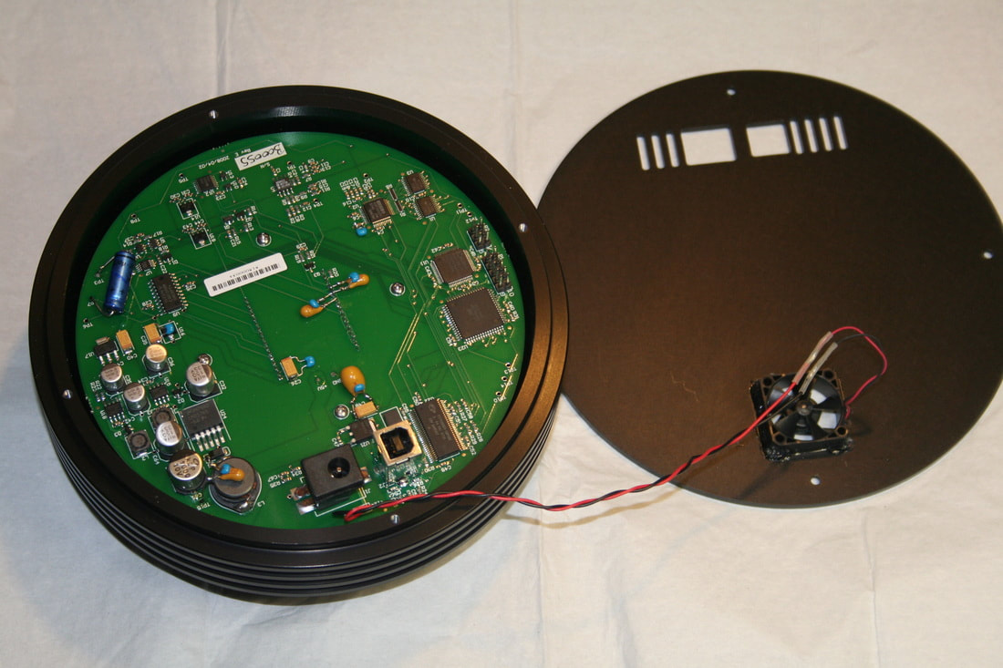
The back cover comes off by removing four screws.
|
|
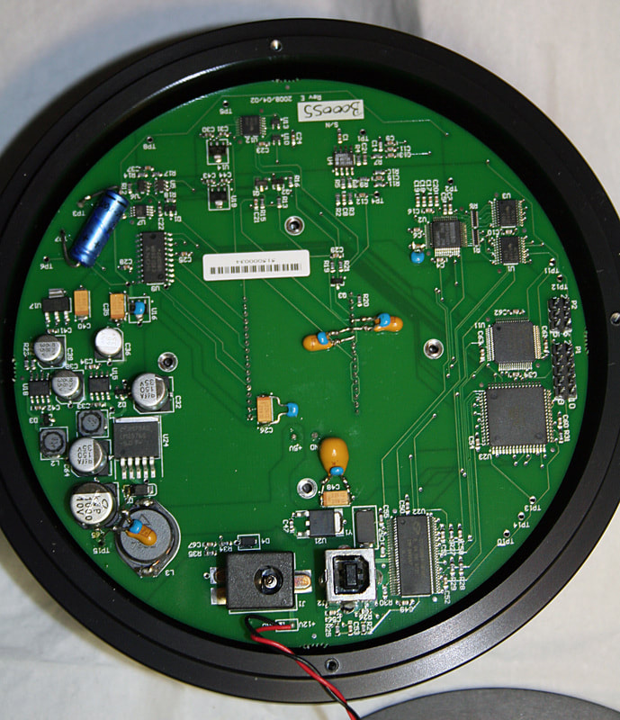
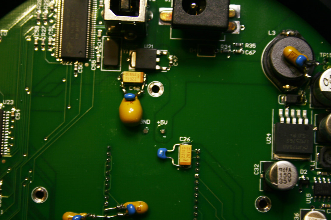
Close up os component side of PCB.
|
|
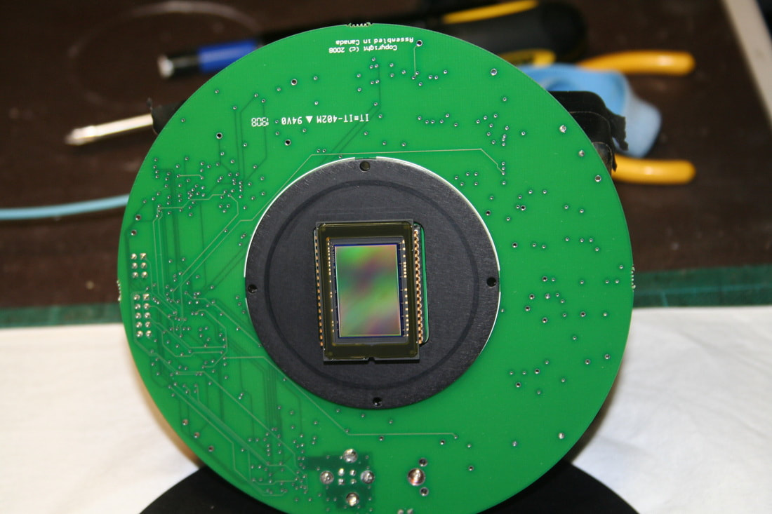
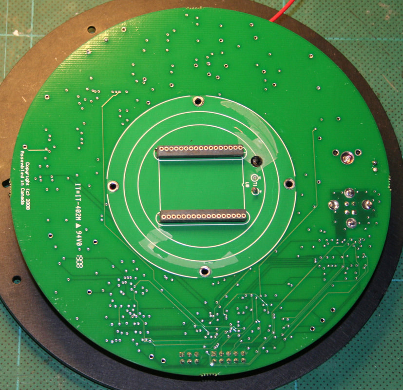
This is the underside of the PCB with the 6 Megapixel sensor. The PCB lifts out after removing the four screws around the sensor (the four holes visible around the edge of the black disk).
This appears to be an 8-layer PCB. I can see 4 trace layers, plus there appear to be power planes and ground planes, and another circular ground plane under the CCD cold plate. The board markings indicate the PCB was manufactured by Introlines Industries of Hong Kong. |
|
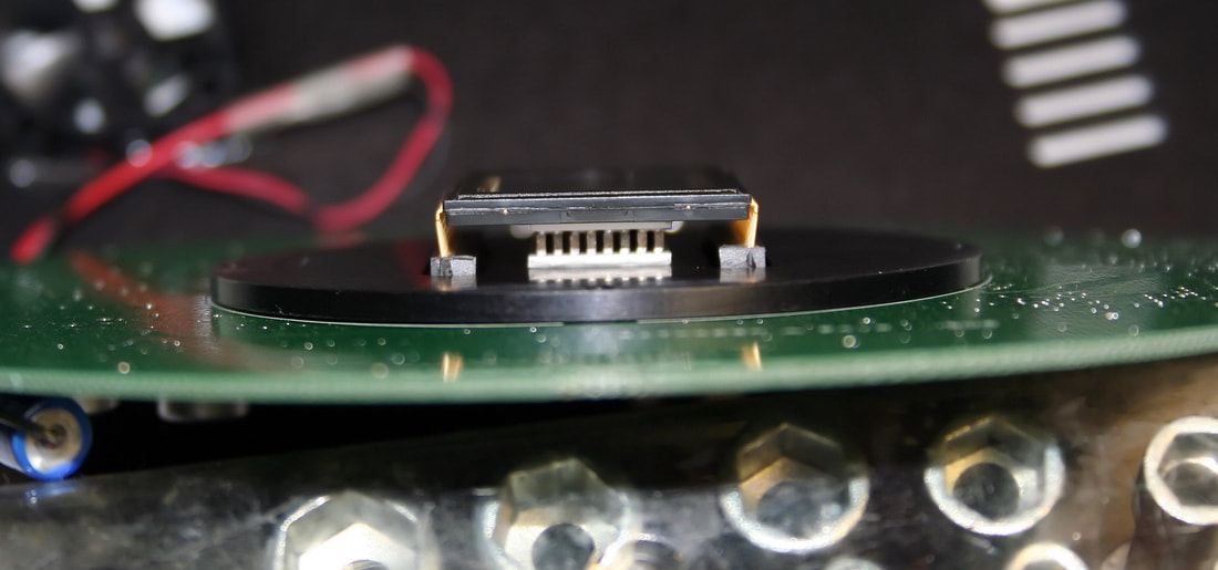
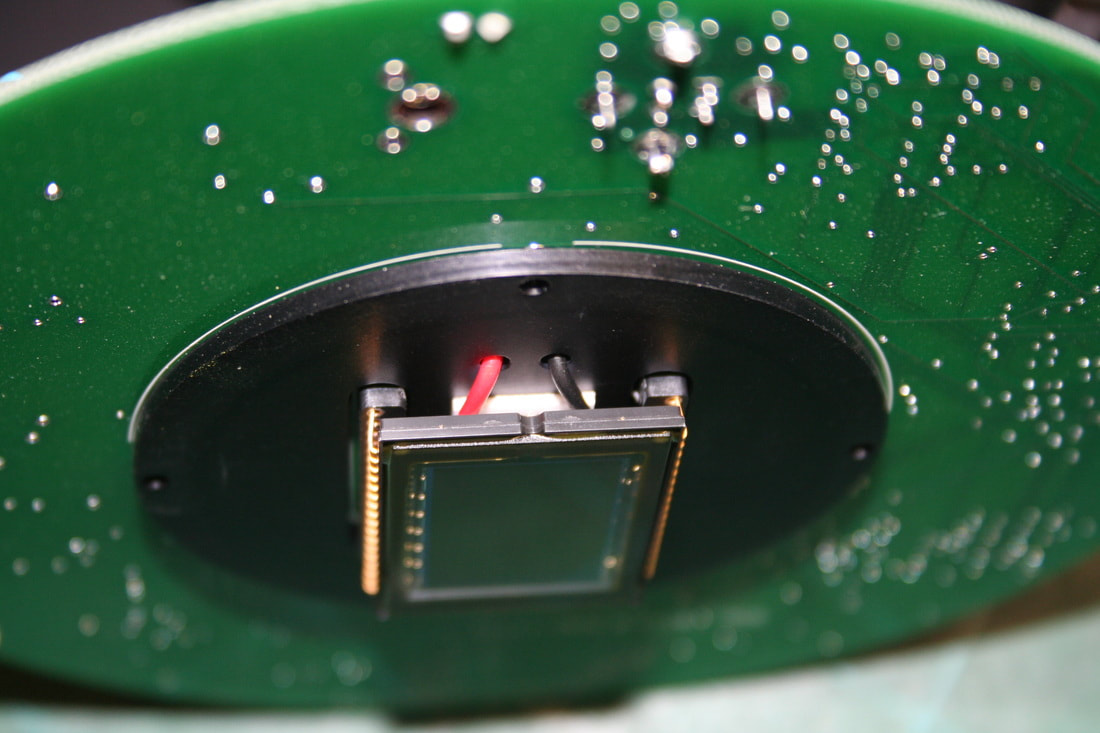
Edge view showing the sensor and peltier device (TEC), and how the TEC is sandwiched directly between the CCD and heatsink.
|
|
On the opposite end of the CCD sensor is the TEC wiring. Black is GND and red is +5VDC.
|
|
The TEC power connects to the two through holes in the PCB labeled +5V and GND near the center of the picture.
|
|
Full view of the sensor side of the PCB with theCCD/TEC/cold plate assembly removed.
|
|
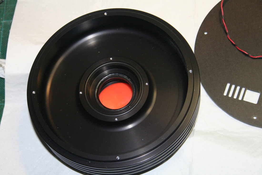
The machined camera housing.
|
|
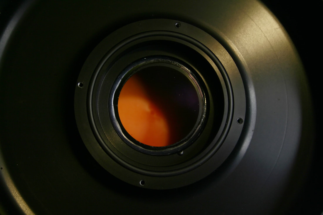
A closer view of the CCD window and o-ring gasket. The chamber window is glued in place. The o-ring sits in a machined groove.
The o-ring forms a seal for the CCD chamber when the circuit board and heatsink are screwed onto the housing. |
Last updated 6/3/2021
